C-MOS buffer
74HC00
Ever wonder what happens when you start adding digital circuits together, using the output of one as the input of another?
Build this project and find out.
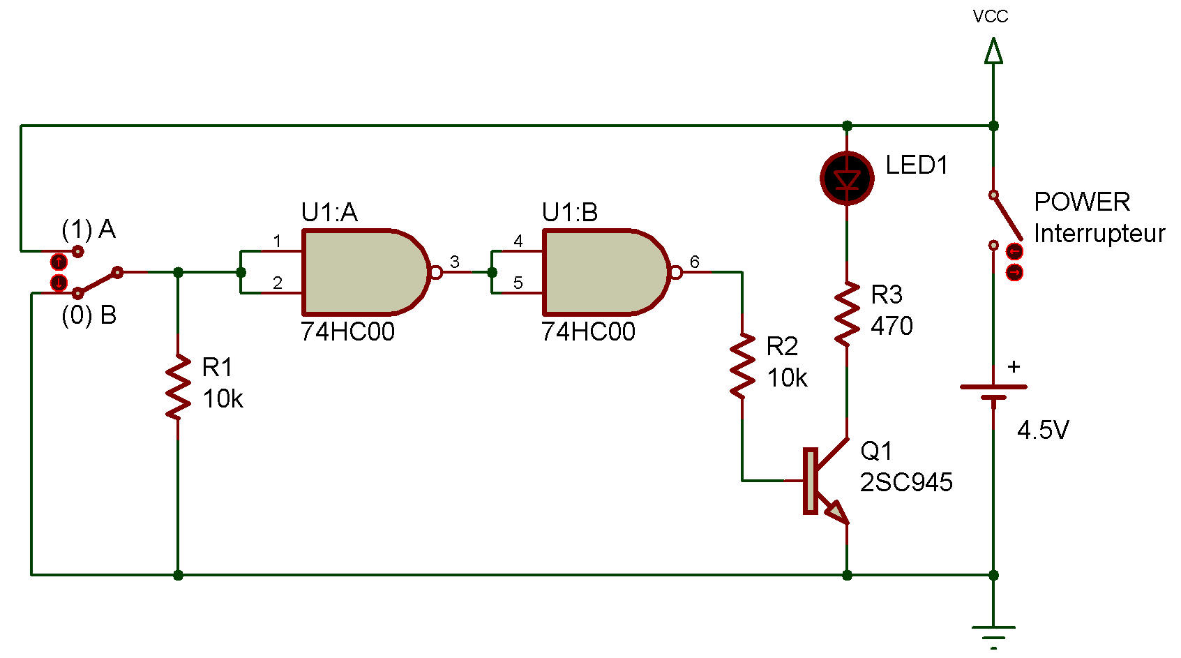
As you can see from the schematic, we take the output from one NAND gate and use it as the input of another: we "split" the output of the first NAND and use it for the inputs to the second (so that the two inputs for the second NAND are the same).
From what you know about NANDs, what do you think happens if the input to the first NAND is 1? If the first input is 0?
Try to figure it out before building this project. After you finished the wiring connection, set the slide switch down. What does LED 1 do?
Now set the select switch up. LED 1 should come on. As you've probably figured out, the input is 1 when the select switch is up, 0 when the select switch is down.
What happens is, when the input to the first NAND is 1, its output is 0. The 0 input to the second causes its output to become 1, lighting the LED. Sometimes we use buffer circuits to simply keep two portions of a device isolated from each other. This type circuit does that job well.
One of the amazing things to think about is how large the RTL and DTL circuits were that we played with in earlier projects. Believe it or not, four circuits like that have been shrunk down to fit inside that tiny IC!
There's even a special type of IC, which are actually computers shrunk to miniature size. They're called microprocessors. The process which lets us several circuits inside just one IC is called large-scale integration, or LSI. You'll see this term often used describe ICs.

![]()